
PCB board
PCB boards are made to speed up the manufacturing of electronic boards . In the past, parts were used in a box and using a large number of wires to connect them, which caused many problems in electronic devices. Today, with the progress of the electronics industry, the need was felt to have a non-conductive plate on which electronic components such as capacitors and ICs can be placed and electronic connections can be established between them. Therefore, printed circuit boards with these features were designed and produced.
Before the pcb board came into existence , the parts were placed in a box and their bases were connected by wires. The communication paths between the bases of electronic components were long and many copper wires were used to connect the bases of the components to each other. This type of construction brought many failures, for example, the loss of the insulation of the wires due to rotting led to the failure of the device. Also, this work caused uncertainty in the circuit and increased complexity in the circuit. With the passage of time and the advancement of pcb board technology, it came into existence, which caused solder to be used instead of many wires to connect the parts.
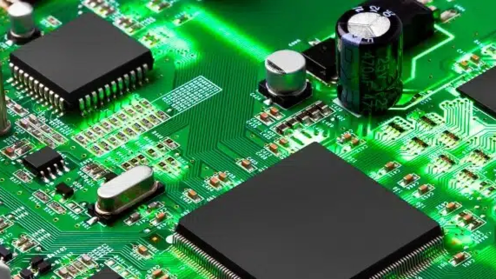
PCB stands for printed circuit board. The printed circuit board consists of a non-conductive board that is covered by a surface of copper, which is used instead of wires for communication between the electronic components of the circuit.
Electronic components such as capacitors, resistors, ICs are installed on PCB and used in electronic equipment, this process is called electrical board assembly.
The role of electronic boards (PCB) in the car
Parts such as car sensors, GPS positioning system, lighting system, door switch modules, engine control section, audio system are all part of the main components of a car that deal with electronics and electronic circuits. Therefore, their functional mechanism depends on the use and design of electronic boards (PCB). PCB in the car has reached significant developments such as the following.
- Improving the performance and efficiency of the fuel system
- Reliable safety and security system that reduces traffic accidents. Electronic boards are abundantly found in systems such as airbag protection system, monitoring, cameras, obstacle detection sensors, etc.
- The evolution of strategic and environmentally friendly programs has led to the production of electric and self-driving (driverless) cars
Different types of boards (PCB) in the car
Boards with high strength: (Rigid Board): These boards are made of solid laminates such as FR4, Rogers, etc. You can see such boards in the car in the displays and rear camera.
Flexible boards : (Flex Circuit): These types of circuits have a flexible structure for installing electronic components used on them. These boards can be bent and twisted, so they will be suitable for corners and curved places. This type is also used in the car for display and broadcasting system.
Boards (Rigid-Flex) : Rigid-Flex boards give the ability to have the two features mentioned above in one board. For example, it will be useful in the lighting system.
PCB boards for LED : In today’s modern cars, high-power LEDs, of course, need bright boards and PCBs that have a high heat exchange. A metal structure such as aluminum is used in these boards. Examples of these boards are used in brake lights, headlights and turn signals.
Boards with a lot of copper : the inner and outer layers of these boards contain 3 ounces or more of copper. These hand boards are used in vehicle safety systems and sending signals.
Key points in PCB design with automotive applications
The PCB designed by you must comply with the relevant standards in order to have acceptable quality and accuracy. Undoubtedly, following the exact process in accordance with the standard and key points of PCB design will prevent serious problems during the production and operation of the board. Therefore, be sure to include the following important points in your design.
1- Direction and placement of parts
The position and placement of parts on the board has a significant impact on the reliability, production and performance of the board. Therefore, it is necessary to follow the procedure below.
- Place similar pieces in the same direction. This will make routing and assembling parts easier.
- For wave soldering, the parts must be created parallel to the wave. This prevents the connection from opening and not soldering properly.
- Do not forget the proper distance between the inductors on the board.
- To avoid crosstalk, place the inductors at right angles to each other.
- Arrange your largest and most important pieces first.
- Separate analog and digital parts in different parts of the board.
- Avoid placing and arranging long components such as electrolytic capacitors in the vicinity of smaller and shorter capacitors. This prevents the soldering from becoming defective and loosening.
- Place parts that consume more power as far as possible from other parts. This will cause more thermal damping from the board.
2- Management of arrangement of parts to avoid coupling
Unprincipled arrangement can affect the magnetic coupling and may cause mutual inductance. The following rules can be used to prevent these effects.
- Avoid placing leads close to each other.
- Place the return flow path close to the main flow path with minimum radiation. By doing this, the current loop path can be reduced.
3- Routing of signal paths in car PCBs
Use 2 to 4 vias per layer to connect layers that have a high current. This will increase reliability, reduce resistance and induction losses, and improve heat exchange. You can use the following rules for routing signals.
- Place the power and GND planes in the inner layers.
- Protect sensitive signals from noise sources with a plan and ensure impedance control for the transmission line.
- Use the shortest and smoothest cracks as possible.
- Use the path of cracks in two-layer boards on one side vertically and on the other side horizontally.
- Use the vertical and horizontal paths mentioned earlier alternately for laminated boards.
4- Optimum heat management
Use proper thermal management techniques for heat dissipation for components that absorb more than 10mV or conduct more than 10mA. The following points can be used for better temperature control.
- Choose copper planes and signal vias as thermal paths to increase heat exchange.
- Place the signal vias near the component with surface pins or under SMD components.
- Use a heat sink for high power components.
- Place thermal copper pads under the hot parts of the board.
- Vaya can be used to transfer heat from thermal surface pads to the ground.
5- Repeated review of design rules
Use the Design Rule Check or DRC to find errors in your design that may not meet your requirements. These can include the following.
- Check proper component spacing for the entire circuit and PCB and individual layers.
- Leave a gap between the power supply and the ground wires and plenty of space between the ground tracks.
- Check for proper ground connection for digital and analog side circuits.
- Make the layout connections in the schematic and PCB correctly.
- Check signal integrity, power integrity, electromagnetic interference and safety requirements.
6- Car design standards
A compact PCB helps to implement information systems, communication, safety, driver assistance systems, engine, etc. As automotive technology continues to advance and move toward driverless cars, the complexity of automotive PCB design also increases. Therefore, for a basic and durable design for electronic boards of cars, follow the standards of IATF 16949, AEC-Q100 and ASE J3016_201401.
7- Grounding the pad of THD parts
The installation holes must be covered and ground. Poor impedance of various circuits is one of the problems. This is mainly due to different electronic components and their connections. Therefore, the following points can be used for the design of electronic boards (PCB) in the car.
- Place the inductance pieces in the sensitive areas near the through holes.
- Use suitable filters that depend on the passing holes.
- Use thinner copper on layers. This reduces the effect of parasitic inductance through the hole on the PCB.
دیدگاه شما چیست؟